Processors compared: Qualcomm Snapdragon 855 vs HiSilicon Kirin 980 vs Samsung Exynos 9820 vs Apple A12 Bionic
We’re at the very end of 2018, and as is the norm, every passing year means a leap ahead on the technology front. The past 12 months have been no different, and the realm of mobile computing platforms have advanced as expected. This year, we have finally transcended the 10nm manufacturing architecture for mobile SoCs, and migrated to even more sophisticated die. HiSilicon, Huawei’s chipset division, was the first to strike blood in terms of the next-generation SoCs, with the Kirin 980 — incidentally also the world’s first 7nm-fabricated SoC. Apple followed suit very closely with its A12 Bionic processor — also built by TSMC (the same manufacturer that made the Kirin 980). Samsung’s announcement came about a couple of months later, when it announced its own, 8nm-based Exynos 9820. Qualcomm, the market leader of mobile SoCs worldwide, dropped in last, taking the wraps off the Snapdragon 855 platform — also built on the 7nm process.
While all these offerings are future-forward and tuned to make the most of technologies slated to steal headlines in 2019, there are a few key differences that set each of them apart. While we could not get hold of an engineering sample and an adequate test rig for each of the chipsets to be tested, we decided to take a look at how they fare against each other in terms of performance, connectivity, imaging, advanced task loads and more, on paper at least. So without further ado, let’s begin.
Round one: Performance
Qualcomm Snapdragon 855
The Qualcomm Snapdragon 855 platform uses eight cores, arranged in a tri-cluster configuration. All the cores used here are Qualcomm’s latest generation of the Kryo cores, which actually feature a semi-custom design, taking reference from existing design from ARM’s cores. In the three-cluster arrangement, the first cluster uses four Kryo 485 ‘silver’ cores, based on older ARM Cortex-A55 cores at the peak speed of 1.8GHz. These are aimed at taking care of all the regular, mundane operations. The second cluster uses three Kryo 485 ‘gold’ cores, which are based on ARM’s latest generation Cortex-A76 cores, and are clocked at up to 2.42GHz. This cluster will be used in slightly more intensive tasks such as casual gaming, or aid heavy AI applications. The third cluster, interestingly, comprises a single core — one Kryo 485 ‘prime’ core, with its peak clock speed unlocked till 2.84GHz. It is, as is obvious, a specialised core for very heavy resource-consuming tasks.
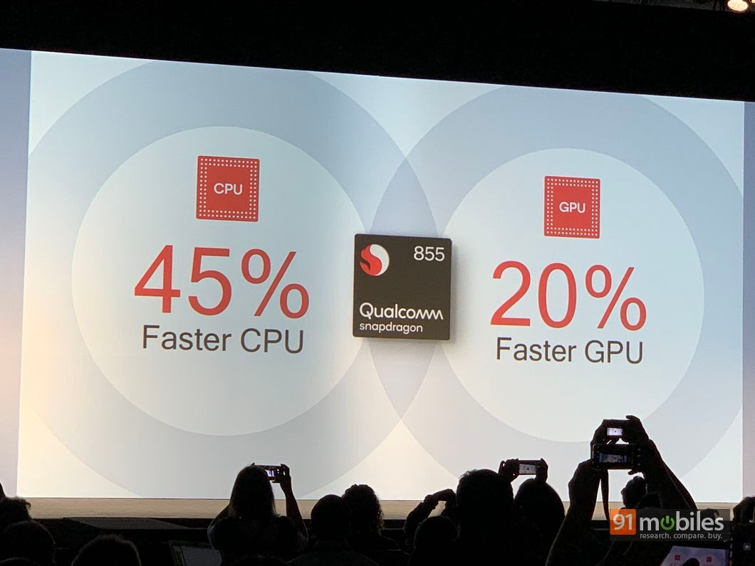
The tri-cluster processor is based on TSMC’s 7nm FinFET manufacturing process, which increases transistor density in a processor. The result is a 45 percent increase in performance over the Snapdragon 845. The core processing assembly is supported by the Adreno 640 GPU, which reportedly renders 20 percent faster graphics than the Adreno 630 GPU. In terms of AnTuTu performance benchmarks, the Snapdragon 855 is said to have breached the 360,000 points mark, and set a new record in terms of performance and speed.
Apple A12 Bionic
The Apple A12 Bionic SoC is a hexa-core, dual-cluster processing platform that was launched with the iPhone XS, XS Max and iPhone XR on September 12th, 2018. It is also the only of the four processors here to have two clusters (all of the rest have three), and has the least number of cores. In terms of cores, it follows a similar architecture as last year’s A11 Bionic, using two, high-performance Vortex cores with a peak clock speed of 2.5GHz, which the company also claims offers increased performance by 15 percent, and efficiency by a more sizeable 40 percent. The other four Tempest cores are 50 percent more efficient than before, and are clocked at 1.6GHz. AnTuTu benchmark scores rank Apple’s SoC to be as fast as the Qualcomm Snapdragon 855, with very minimal differences between the two.
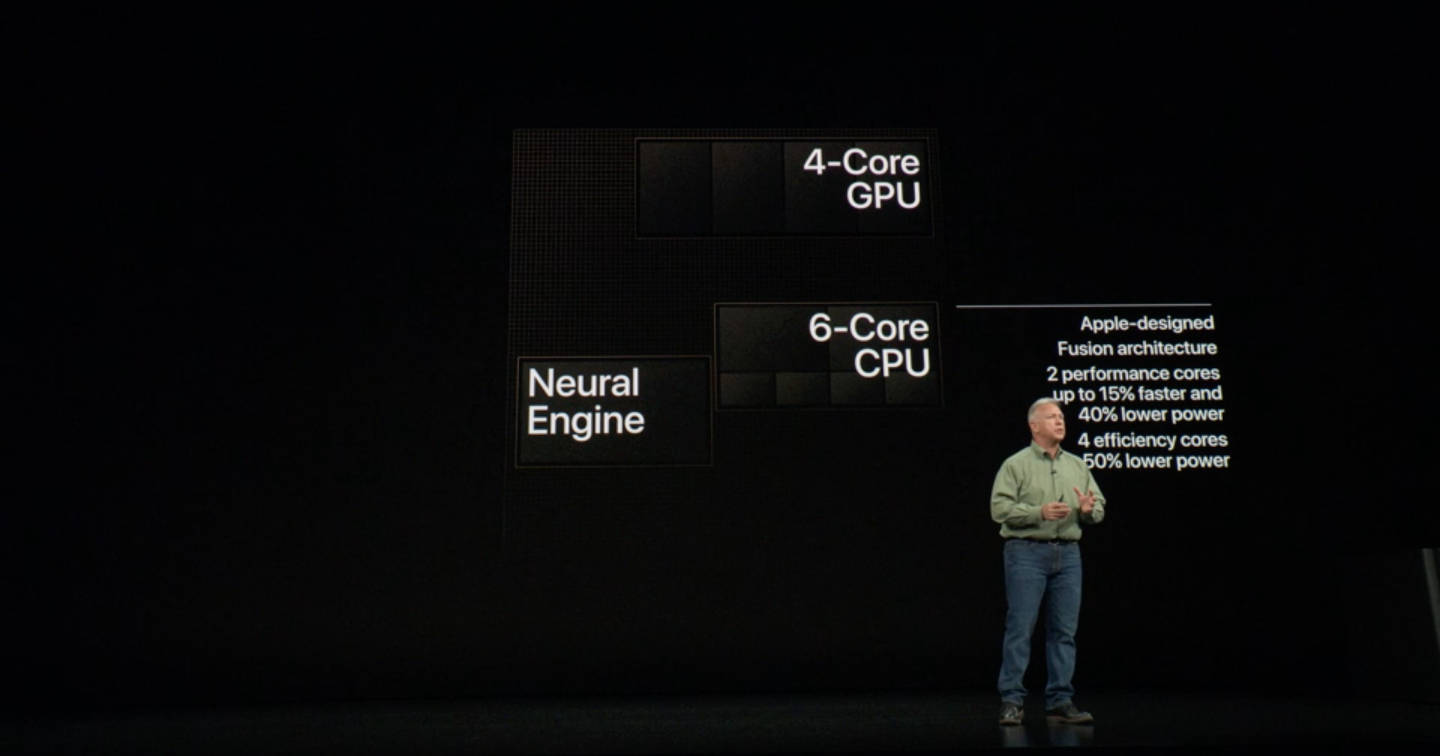
This is further complemented by two elements — Apple’s custom, quad-core GPU and an octa-core neural processing unit (NPU), both acting as active co-processors to share processing load with the main CPU. Importantly, all six of the CPU’s cores cannot work at the same time. The GPU is custom-built by Apple, and is reportedly 50 percent faster than the previous-gen graphics unit, which provides a sizeable jump in terms of graphics processing. It also provides features such as multi-layer rendering and lossless memory compression. Essentially, instead of presenting the A12 Bionic as a package, Apple has distributed the workload among separate sections of the processor. For instance, all AI and ML-related operations are handled by the NPU, which is discussed in the subsequent section.
Samsung Exynos 9820
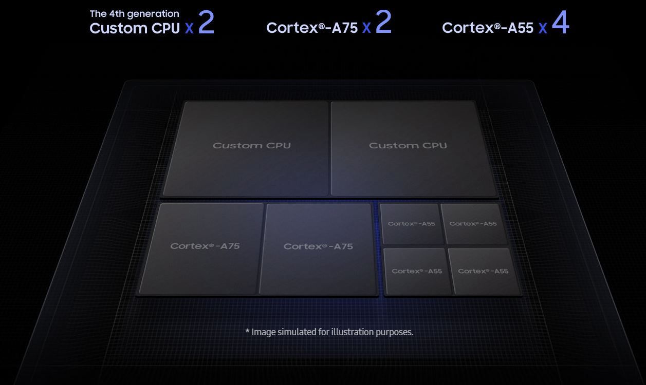
Samsung’s System LSI division has been churning out its own, custom ARM-based processors for a while now, of which the latest iteration comes with a slightly inferior 8nm FinFET fabrication process, in comparison to the 7nm process used by the rivals. The Samsung Exynos 9820’s 8nm LPP (Low Power Plus) architecture reportedly facilitates 15 percent more performance, at 10 percent lesser power consumption, which theoretically can never be a bad thing. Its tri-core architecture uses a 2+2+4 configuration, with the four mainstream cores being ARM Cortex-A55 cores of unspecified peak clock speed. The two mid-performance cores are Cortex-A75, again of unspecified clock speed. Finally, the two main ‘big’ cores are Samsung’s custom-built Mongoose M4 cores. Presumably, while the Mongoose cores will chase peak performance, the A55 cores are built to maximise efficiency. In terms of benchmarks, the Exynos SoC scores around 325,000 points, which seems to be a fair reflection of real-life performance.
Contrary to expectations, Samsung did not opt to build its own GPU. Instead, it continues its partnership with ARM, and has equipped the Exynos 9820 with ARM’s Mali G76 GPU. The new G76MP12 unit now has 12 graphic execution units, up by 33 percent over last year, and the Chaebol claims that this has helped it improve increase performance by 40 percent with the same power supply, or increase 35 percent efficiency the at same performance levels, when compared to the last year’s GPU. It supports all popular codecs, and renders 4K videos at up to 150fps. This makes it reasonably fast, but not as fast as Qualcomm’s and Apple’s GPUs.
HiSilicon Kirin 980
The Kirin 980 was technically the very first to have launched with TSMC’s 7nm FinFET process. As such, it also became the first in the world to use a Cortex-A76 core, the newest member in ARM’s arsenal, and also pushed the connectivity barrier (although that has already been undone). The Kirin 980 works in a 2+2+4 architecture that is actually closer to the Snapdragon 855’s configuration, than that of the Exynos 9820. The two ‘big’ cores utilise A76 cores with the clock speed of 2.6GHz, while two more A76 cores have been put in place (at the risk of taking up more space in the die) to handle medium-intensity tasks, and are clocked at 1.92GHz. The four ‘little’ cores here use Cortex-A55 cores and run at 1.8GHz clock speed, and use ARM’s latest DynamIQ CPU controller. This has allowed HiSilicon to effectively tweak throughputs, thereby being better at efficiency and power management than before. AnTuTu scores peg it at around 310,000.
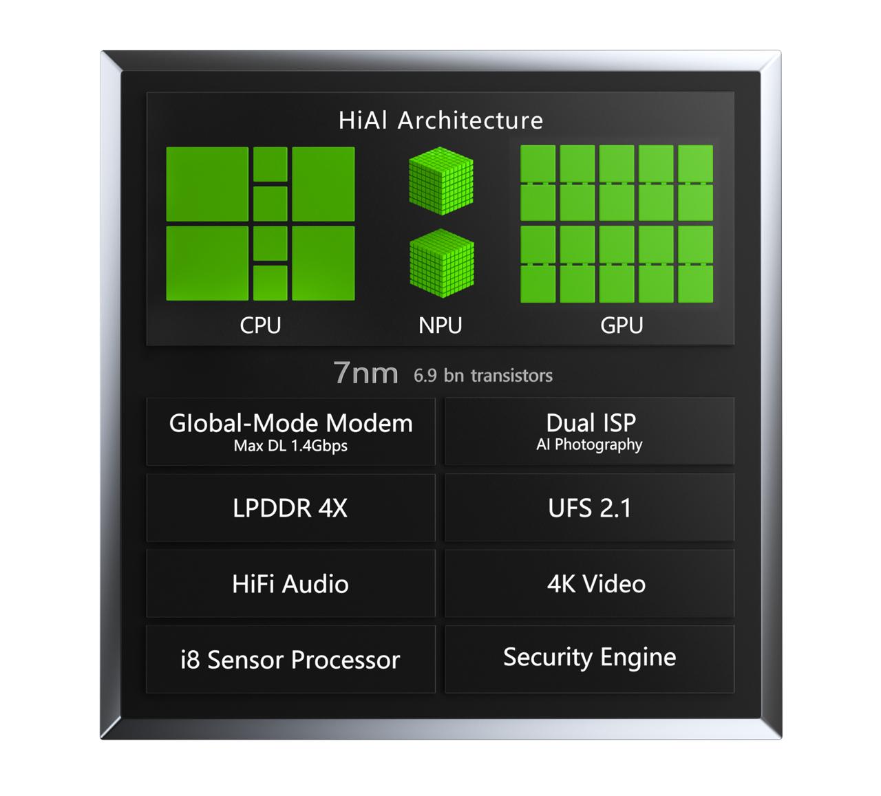
The Kirin 980 was also the first to use Mali’s latest G76 GPU, but uses 10 execution points in comparison to Samsung’s 12 (although this one is clocked marginally higher than Samsung’s). It remains to be seen how this plays out in real life, but Huawei has noted that the G76 GPU provides 46 percent performance increase over its predecessor, and a rather tall claim of 178 percent lesser power consumption. It has also stated that the GPU is now compatible with Huawei’s AI frequency modulation scheduling, which is a fancy name for intelligent task efficiency management. The company has claimed 30 percent better graphics rendering in terms of mainstream usage, and smooth 60fps gaming as well.
Round two: AI and advanced tasks
Qualcomm Snapdragon 855
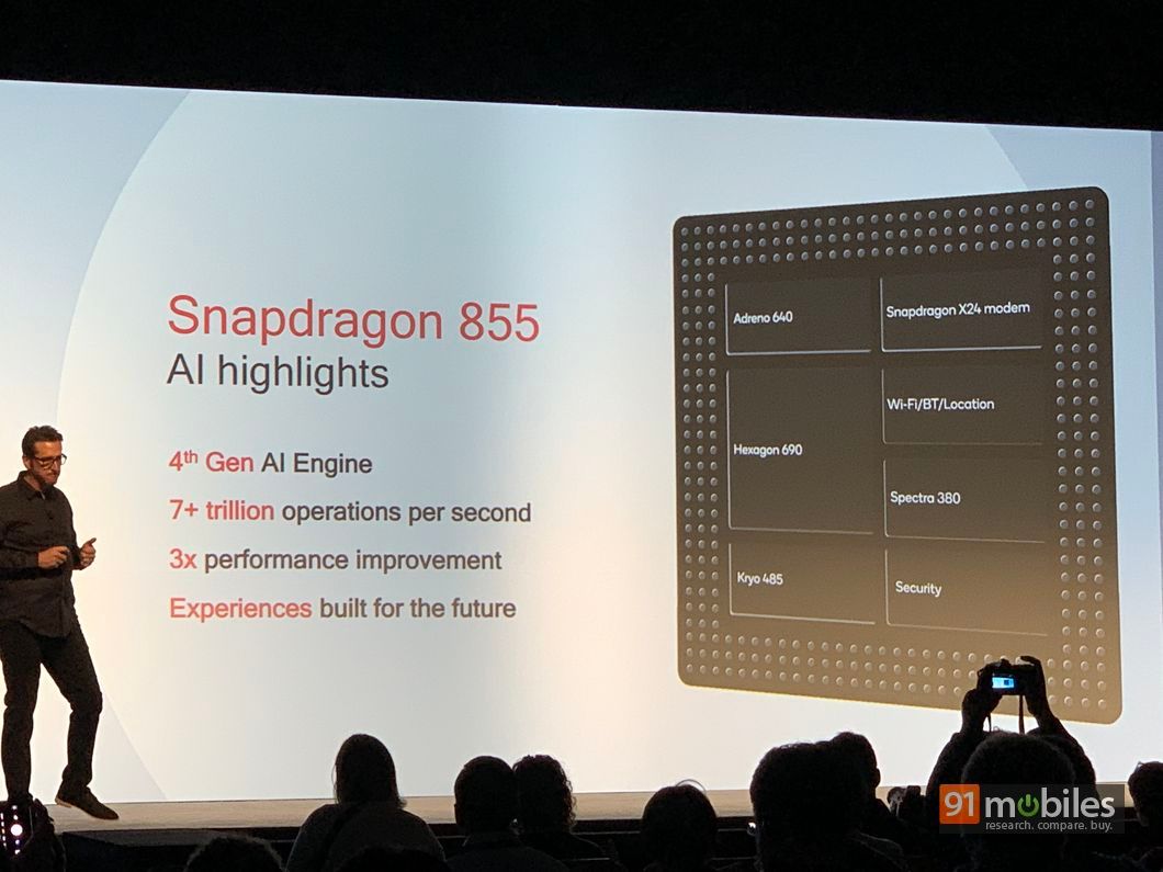
To take on artificial intelligence-enabled features, the Snapdragon 855 is equipped with the Hexagon 690 digital signal processor (DSP). This acts as an AI co-processor, wherein any heavyweight AI task can use either the CPU, the GPU or the DSP, or even a combination of them, to execute the task. The Snapdragon 855 gets four vector accelerator pipelines, accounting for a 20 percent increase in overall performance of heavy, specialised tasks. It also gets a new Hexagon Tensor Accelerator (HTA), which is Qualcomm’s first neural network and machine learning inferencing engine. This would make a massive difference in the computation of AI tasks. It also includes support for Snapdragon Neural Processing development kit, the Hexagon Neural Network and a host of popular neural networking frameworks. All of this not only makes the Snapdragon 855 a faster overall processor for advanced tasks, but also a more future-proof option than before.
Apple A12 Bionic
The A12’s neural engine, codenamed Quin, quotes massive processing power of 5 TFLOPS (trillion floating point operations per second), up from the 600 billion FLOPS that the A11’s neural engine was capable of. It also gets multiple data precision points, which in layman terms is crucial for deep neural networks to operate at blazing fast speeds. For instance, this is what enables features such as Apple’s Face ID and Animoji to work without latency, and the A12 SoC increases the further potential for the present iPhones. It also gets a smart compute system, which allows it to dynamically assign compute cores to required tasks. This is how Apple manages heavy tasks, making its neural engine and the GPU share much of the CPU’s workload.
Samsung Exynos 9820
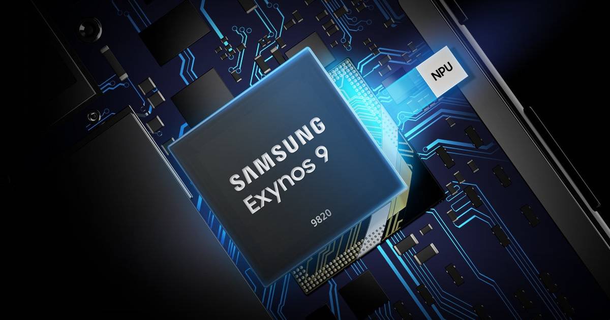
While details are severely scarce on the ground, Samsung has stated that it does use an NPU to aid performance, as well as take care of AI-related tasks. All we know so far is that it will be ‘7x faster’ in AI-based and other heavyweight tasks, in comparison to the Exynos 9810. That, though, does not say a whole lot about it, so we’ll hope that Samsung’s NPU holds up in tasks such as photography enhancements, and AR rendering.
HiSilicon Kirin 980
The Kirin 980 reportedly includes a dual NPU, while in essence it actually handles one kernel at a time, but is scaled to handle two. On paper, it’s twice as fast as the Kirin 970’s NPU, and has also posted significantly higher image inference numbers in comparison to the older generation SoCs from Qualcomm and Apple. What this means in real life is reliable AI and ML operations, much smoother overall performance from Kirin 980-equipped devices, and the prospect of facial recognition with 3D ToF hardware.

Round three: Imaging
Qualcomm Snapdragon 855
Imaging in the Snapdragon 855 SoC is primarily taken care of by the Spectra 380 image signal processor (ISP), which is a significant improvement over its predecessor. The company claims the Spectra 380 to be the world’s first computer vision ISP on mobile, theoretically preparing it for a huge host of advanced tasks such as advanced object recognition, heavy AR rendering and even augmented interactions. It also uses power from the Kryo cores, the GPU and the DSP to aid processing speeds, freeing up space for much more imaging features. The result of all this is support for up to two 22-megapixel sensors (or a single 48-megapixel one), and features such as enhanced background defocus, object segmentation in images, 4K HDR10+ videography at 60fps, and real-time background swap.

Apple A12 Bionic
Apple’s dedicated ISP, codenamed Petra, does not provide as much painstaking detail as the other chipmakers do. However, much of Apple’s computer vision functions are handled by the neural engine, with the ISP sharing its workload with it. However, it is the least impressive of the lot in terms of photography, supporting a maximum of two 12-megapixel sensors. In terms of videography, while it does manage 4K shooting at 60fps, it is not as impressive as Qualcomm and Samsung’s efforts. Apple however, does state that it has calibrated its camera for AR operations at 60fps in low light, and it also comes with a faster depth engine for better portrait mode photographs.
Samsung Exynos 9820
There is not a whole bunch of detail about the ISP’s architecture, but the Exynos 9820 makes fairly tall claims when it comes to imaging prowess. The ISP supports up to two 16-megapixel sensors, or one 22-megapixel shooter. In fact, the Exynos 9820 has made the most impressive of all imaging claims among these processors, stating that the media encoder in the Exynos SoC can support up to 8K HDR videos at 30fps, or 4K HDR at a staggering 150fps. This does hint at a pretty well-equipped camera, hopefully slated for the Galaxy S10 series. Interestingly, there is also integrated support for up to five camera sensors, with the Exynos 9820. We wonder if that’s a bit of a hint at something.
HiSilicon Kirin 980
The new ‘dual ISP’ onboard the Kirin 980 is, yet again, significantly better than before. This is a good thing, since Huawei has been gunning for Leica lenses and ridiculously high megapixel count in cameras for a while now. Apart from the claim of 46 percent higher image processing speed and 23 percent video shooting power efficiency, the Kirin 980 also has the most superior sensor support, going up to 40-megapixel single-sensor support, or two sensor arrays at 40-megapixel and 20-megapixel sensors. The video encoder can unfortunately only support 4K videos at 30fps, which is a bit of a shame. Nevertheless, it also gets 10-bit HDR pipeline and inter-frame noise reduction, which will produce sharper photographs with more accurate colours, and take lesser time than before.
Round four: Connectivity
Qualcomm Snapdragon 855
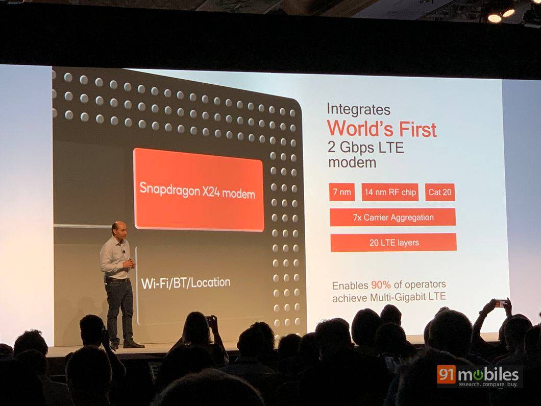
The Qualcomm Snapdragon 855 brings 5G to the forefront, with the optionally configurable X50 5G modem. This modem brings support for both sub-6 and mmWave 5G networks, thereby entailing network speeds of up to 5Gbps at heavily reduced network latency. Beyond the 5G compatibility, the Snapdragon 855 includes features such as WPA3 network security, 67 percent lesser power consumption, 8×8 sounding for more simultaneous connections, up to 10Gbps Wi-Fi speeds, 2Gbps Cat.20 LTE speeds with the X24 LTE modem, and effective upload speeds of up to 316Mbps. This provides a solid, overall improvement in network speeds, hence providing potential devices the theoretical capability of seamless multi-device connections, low latency synchronisation and smooth inter-connectivity, which can be crucial in the IoT scheme of things.
Apple A12 Bionic
To be entirely honest, there isn’t anything of exceptional noteworthiness about the A12 Bionic’s connectivity chops. It uses an Intel XMM7560 modem, which in fact is a matter of great dispute (Qualcomm is gunning for iPhone bans based on alleged intellectual property infringement by Apple). It is capable of 1Gbps LTE speeds, and while that is nowhere close to the Wi-Fi network advancements, or higher LTE capabilities of the Snapdragon 855, has proved to be reliable and functional in real life. Where it will lose out, however, is in the future, when faster networks do become available. There are no optional 5G modems either, and Apple isn’t expected to announce one until at least 2020.
Samsung Exynos 9820
While the Exynos 9820 SoC does not have the 5G razzmatazz happening for it, there is a pretty robust 4G LTE modem that matches LTE download and upload speeds specified by the Snapdragon 855. It uses its own Cat.20 LTE modem, producing 2Gbps LTE speeds and 316Mbps uploads, along with mass carrier aggregation technology onboard, that should improve network reception in congested or low coverage areas.
HiSilicon Kirin 980
Before it was outdone by the Exynos 9820 and the Qualcomm Snapdragon 855, the Kirin 980 hit the charts with the Cat.21 LTE modem. This pushed the 1Gbps LTE speeds up to 1.4Gbps, which simultaneously pushed upload speeds to 200Mbps. It also gets 3x carrier aggregation technology, which should work fairly well. Furthermore, HiSilicon did speak about an extra 5G modem — the weirdly-named Balong 5000 modem. That said, all we know about it is that it can be an accompanying module in future Huawei and Honor devices, and can be used when the networks are ready to be deployed.
Summing it up
To sum up, the four behemoth processors are truly going for the kill when it comes to performance, graphics, artificial intelligence, imaging and connectivity. This makes 2019 an exciting year ahead in terms of smartphone performance, and what remains to be seen is whether we do end up with functionalities and network infrastructure to make use of all the fantastic bits of technology stored in these chips.
In terms of our comparison, it certainly isn’t conclusive to judge through an on-paper comparison. However, HiSilicon appears to have improved in major leaps, and Huawei’s recent phones do seem quite enticing. Qualcomm will be firing the big guns, but Apple already has a fierce competitor in its own hands, which will probably only slightly be outrun. While the Exynos processor is quite good as well, it may not be as powerful, efficient or wholesome as Qualcomm and Apple’s solutions.
Do you think these SoCs will function as per their claims? Will we be in for any big shocker, and which one will outperform one another? Let us know what you think, while we wait for 2019’s smartphones to start rolling in to pit them against each other.
from 91mobiles.com http://bit.ly/2GM2kZZ
>


No comments